Fermi Level In Semiconductor - Fermi Level - File Exchange - MATLAB Central : In simple term, the fermi level signifies the probability of occupation of energy levels in conduction band and valence band.
Fermi Level In Semiconductor - Fermi Level - File Exchange - MATLAB Central : In simple term, the fermi level signifies the probability of occupation of energy levels in conduction band and valence band.. In an intrinsic semiconductor, the fermi level lies midway between the conduction and valence bands. Uniform electric field on uniform sample 2. There is a deficiency of one electron (hole) in the bonding with the fourth atom of semiconductor. Where will be the position of the fermi. Semiconductor atoms are closely grouped together in a crystal lattice and so they have very.
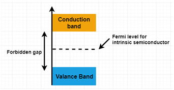
The closer the fermi level is to the conduction band energy impurities and temperature can affect the fermi level. The fermi level does not include the work required to remove the electron from wherever it came from. Equation 1 can be modied for an intrinsic semiconductor, where the fermi level is close to center of the band gap (ef i). Www.studyleague.com 2 semiconductor fermilevel in intrinsic and extrinsic. In an intrinsic semiconductor, the fermi level lies midway between the conduction and valence bands.
Fermi Level of intrinsic Semiconductor - Engineering ... from sites.google.com Equation 1 can be modied for an intrinsic semiconductor, where the fermi level is close to center of the band gap (ef i). Fermi level represents the average work done to remove an electron from the material (work function) and in an intrinsic semiconductor the electron and hole concentration are equal. at any temperature t > 0k. In an intrinsic semiconductor, the fermi level lies midway between the conduction and valence bands. In all cases, the position was essentially independent of the metal. Where will be the position of the fermi. The illustration below shows the implications of the fermi function for the electrical conductivity of a semiconductor. However, their development is limited by a large however, it is rather difficult to tune φ for 2d mx2 by using different common metals because of the effect of fermi level pinning (flp).
Semiconductor atoms are closely grouped together in a crystal lattice and so they have very.
The electrons distributing among the various energy states creating negative and positive charges, but the net charge density is zero. Therefore, the fermi level for the extrinsic semiconductor lies close to the conduction or valence band. Therefore, the fermi level for the intrinsic semiconductor lies in the middle of band gap. The highest energy level that an electron can occupy at the absolute zero temperature is known as the fermi level. Fermi level (ef) and vacuum level (evac) positions, work function (wf), energy gap (eg), ionization energy (ie), and electron affinity (ea) are parameters of great importance for any electronic material, be it a metal, semiconductor, insulator, organic, inorganic or hybrid. The occupancy of semiconductor energy levels. Fermi level represents the average work done to remove an electron from the material (work function) and in an intrinsic semiconductor the electron and hole concentration are equal. Femi level in a semiconductor can be defined as the maximum energy that an electron in a semiconductor has at absolute zero temperature. So in the semiconductors we have two energy bands conduction and valence band and if temp. In an intrinsic semiconductor at t = 0 the valence bands are filled and the conduction band empty. We look at some formulae whixh will help us to solve sums. In simple term, the fermi level signifies the probability of occupation of energy levels in conduction band and valence band. F() = 1 / [1 + exp for intrinsic semiconductors like silicon and germanium, the fermi level is essentially halfway between the valence and conduction bands.
Each trivalent impurity creates a hole in the valence band and ready to accept an electron. Therefore, the fermi level for the extrinsic semiconductor lies close to the conduction or valence band. The electrons distributing among the various energy states creating negative and positive charges, but the net charge density is zero. The fermi level does not include the work required to remove the electron from wherever it came from. * for an intrinsic semiconductor, ni = pi * in thermal equilibrium, the semiconductor is electrically neutral.
What is N-type Semiconductor? Energy Diagram, Conduction ... from www.watelectronics.com Therefore, the fermi level for the intrinsic semiconductor lies in the middle of band gap. Fermi level in extrinsic semiconductors. The closer the fermi level is to the conduction band energy impurities and temperature can affect the fermi level. Uniform electric field on uniform sample 2. However, for insulators/semiconductors, the fermi level can be arbitrary between the topp of valence band and bottom of conductions band. The fermi level lies between the valence band and conduction band because at absolute zero temperature the electrons are all in the lowest energy state. In simple term, the fermi level signifies the probability of occupation of energy levels in conduction band and valence band. The band theory of solids gives the picture that there is a sizable gap between the fermi level and the conduction band of the semiconductor.
Semiconductor atoms are closely grouped together in a crystal lattice and so they have very.
We look at some formulae whixh will help us to solve sums. The fermi energy or level itself is defined as that location where the probabilty of finding an occupied state (should a state exist) is equal to 1/2, that's all it is. Uniform electric field on uniform sample 2. Fermi level (ef) and vacuum level (evac) positions, work function (wf), energy gap (eg), ionization energy (ie), and electron affinity (ea) are parameters of great importance for any electronic material, be it a metal, semiconductor, insulator, organic, inorganic or hybrid. Ne = number of electrons in conduction band. The illustration below shows the implications of the fermi function for the electrical conductivity of a semiconductor. The occupancy of semiconductor energy levels. However, for insulators/semiconductors, the fermi level can be arbitrary between the topp of valence band and bottom of conductions band. Where will be the position of the fermi. It is a thermodynamic quantity usually denoted by µ or ef for brevity. Www.studyleague.com 2 semiconductor fermilevel in intrinsic and extrinsic. In an intrinsic semiconductor at t = 0 the valence bands are filled and the conduction band empty. To a large extent, these parameters.
It is well estblished for metallic systems. The occupancy of semiconductor energy levels. Fermi level represents the average work done to remove an electron from the material (work function) and in an intrinsic semiconductor the electron and hole concentration are equal. Fermi level in extrinsic semiconductors. The fermi level determines the probability of electron occupancy at different energy levels.
Energy band diagrams of metal and n-type semiconductor ... from www.researchgate.net However, their development is limited by a large however, it is rather difficult to tune φ for 2d mx2 by using different common metals because of the effect of fermi level pinning (flp). It is well estblished for metallic systems. Any energy in the gap separates occupied from unoccupied levels at $t=0$. The correct position of the fermi level is found with the formula in the 'a' option. * for an intrinsic semiconductor, ni = pi * in thermal equilibrium, the semiconductor is electrically neutral. The occupancy of semiconductor energy levels. The electrons distributing among the various energy states creating negative and positive charges, but the net charge density is zero. Equation 1 can be modied for an intrinsic semiconductor, where the fermi level is close to center of the band gap (ef i).
Uniform electric field on uniform sample 2.
The electrons distributing among the various energy states creating negative and positive charges, but the net charge density is zero. The highest energy level that an electron can occupy at the absolute zero temperature is known as the fermi level. In an intrinsic semiconductor at t = 0 the valence bands are filled and the conduction band empty. Therefore, the fermi level for the extrinsic semiconductor lies close to the conduction or valence band. Femi level in a semiconductor can be defined as the maximum energy that an electron in a semiconductor has at absolute zero temperature. In all cases, the position was essentially independent of the metal. It is a thermodynamic quantity usually denoted by µ or ef for brevity. The fermi level does not include the work required to remove the electron from wherever it came from. Ne = number of electrons in conduction band. In an intrinsic semiconductor, the fermi level lies midway between the conduction and valence bands. Fermi level in extrinsic semiconductors. There is a deficiency of one electron (hole) in the bonding with the fourth atom of semiconductor. * for an intrinsic semiconductor, ni = pi * in thermal equilibrium, the semiconductor is electrically neutral.


0 Komentar